How Does Scanning Electron Microscope work ?
Contents
Features of SEM-6200 Scanning Electron Microscope
Scanning Electron Microscope (SEM) is a large-scale, high precise electron optics instrument used to research microscopic structures of objectives. It receives the stimulated electron signals and forms images by focused electron beam scanning on the specimen surface spot by spot. The machine has following features:
- It has large depth of field, which is applicable to the analysis and observation of rough surface and fracture; the images are stereoscopic and realistic, and easy to be identified and explained.
- It can be used to observe the surface structures of large-scale solid specimens; the diameter of specimen can be up to 15mm; the sample preparation and pretreatment are simple.
- The resolution can be reach to 4.5nm.
- The range of magnification is large; for multiphase and multi-composition nonhomogeneous material, it is convenient for general observation at low magnification and precisely analyzed at high magnification.
- The operation is simple: Users can master it after receiving a short-term training.
- Electronics and computer science can be used to properly improve the quality of image.
- More image observation modes: E.g. Multi Channels can help users observe images from different detectors simultaneously.
- According to the purpose of observation, users can carry out dynamic tests by changing different stages such as high temperature stage, low temperature stage and pulling stage to observe phase transition and transformation under different conditions.
- The extensiveness of the instrument is good; users can carry out multi-function analysis by adding different signal detecting devices, e.g. X-ray energy spectrometer can be used to do micro-area components analysis, or qualitative and quantitative analysis of components in different micro-areas of specimen.
- Windows operating system; the operation interface is friendly, succinct, and easy to master; the image is displayed on the same screen, and can be zoomed out or zoomed in; the maximum image resolution is 4096*4096*24; USB2.0 standard communication interface for the peripheral equipment and supports hot plug.
- The pre-installed image processing software supports multiple universal image formats and the conversion between different image formats; the optional image processing software strengthens a series of image processing functions, such as particle analysis.
Main Purpose and Scope of Application
Scanning Electron Microscope (SEM) can be used for ceramic material analysis and metallic material failure analysis. SEM can also be widely used in other fields such as petroleum, geology, mineral, electron, semiconductor, medicine, biology, chemical industry, macromolecular material, criminology, agriculture and forestry, etc.
SEM can be used for microstructure analysis, and normal micro-area analysis, including quantitative and qualitative analysis of components. For microstructure analysis, spatial
resolution can reach to submicron grade. State measurement of grain boundary, phase identification of crystal/crystal grain, and crystallographic orientations measurement can also be carried out by use of SEM. When making micro-area components analysis, element distribution measurement can be carried out by rapid multi-element mapping and line scan.
In modern industrial production and scientific research, SEM becomes one of the necessary methods of material analysis, industrial and agricultural process control, quality control and safety production. Meanwhile, the application of SEM are changing rapidly in the fields of human survival and development, such as biology, environmental protection and medicine.
Specification and Its Meaning Product
name: Scanning Electron Microscope Product
model: SEM6200
![%}LQ[$HG(8]7)P`FKYH141E](https://fyitester.com/wp-content/uploads/LQHG87PFKYH141E.png)
Using Condition
Environmental Condition
Temperature 22℃±5℃ Temperature change ≤1℃/h Relative humidity ≤70% (25℃)
Floor load ≥246Kg/m
Working Condition
Power Supply
Single-phase 220V±22V, 50±1Hz, 15A power supply Stability of power supply ±5%
Independent ground Grounding resistance ≤4Ω
Caution: it is suggested to equip one set of 3KVA AC voltage stabilizer to avoid the strong disturbance of power network.
Other Working Conditions
Vibration ≤3μm
Space magnetic field ≤ 3m Gauss
Laboratory Floorplan Installation Condition

Electrical Outlet (16A)
Influence on Environment and Energy Sources
The X-ray radiations conform to the national standard, and will not influence environment and energy sources.
Safety
The safety of KYKY-EM6200 conforms to the requirements of the national safety standards of instruments.
Structure Feature and Operating Principle
General Structure of Scanning Electron Microscope
The interaction of between a certain energy electron beam and sample, will produce various physical signals. The SE detector collects and amplifies secondary electronic signal, then transmit the signal to electrics console, converts to digital signal. Finally, the computer receive the signal and form a image. The main structure of SEM6200 are electron optics column, chamber, automatic vacuum system, electronics and display console, etc.
Electron Optics Column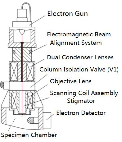
SEM6200 electron optics column can produce and focus electron beam to form a fine spot on specimen. The electron optics column consists of electron gun, electromagnetic beam alignment system, dual condenser lenses, column isolation valve (V1), objective lens, scanning coil assembly, stigmator and electron detector. The system has one set of electromagnetic shielding column outside the optical path, which can eliminate the electromagnetic interference from the environment.
Electron Gun
Electron gun is a high brightness electron source, which is a self-biased triple structure. The filament tip, wehnelt cap hole center and anode hole center are coaxial for the result of highest brightness. The distance between anode and wehnelt cap is adjustable for high or low accelerating voltage. Three screws above electron gun are used to adjust the position of electron gun in order to realize filament alignment (mechanical alignment).
Electromagnetic Beam Alignment System
In daily work, the mechanical alignment can not ensure strict alignment of electron beam, so electromagnetic beam alignment system is also adopted to ensure coincidence of electron beam and the optical axes. The control of electromagnetic beam alignment system can be adjusted by software. (Refer to Section 3.4.12. Control Panel of Basic Function for Beam Alignment.)
Dual Condenser Lenses
Electron optics column includes two same condenser lenses. The pole pieces of the two condenser lenses are installed on the two ends of one cylinder and share one coil. For thereasons of convenient cleaning and vacuum sealing, a metal liner is set in the middle of condenser lens. When working normally, inside the liner is vacuum state, outside the liner is atmosphere. Thus, when cleaning electron optics path, there is no need to disassemble the condenser lens; but only take out the liner for cleaning, and then replace the aperture which is installed under the bottom of the liner. When cleaning, the liner should be drawn out from the top of optical path.
Column Isolation Valve(V1)
Column V1 is a manually operated vacuum valve, which is installed between condenser lens and objective lens. This valve separates column from chamber. So, when replacing specimen, the chamber is in atmosphere, the column can still keep in vacuum state. When opening V1 valve, the high voltage interlock function is started at the same time.
Objective Lens
Objective lens is asymmetrical, with long working distance, low spherical aberration and small magnetic leakage. The bottom pole piece of objective lens can be dismounted without any influence on original state of scanning coil.
The final apertures are installed between top and bottom pole piece of objective lens. Three apertures can be installed in the final aperture holder, diameter of aperture is usually 100μ m or 200 μ m (customers can choose other diameters according to actual needs). The
X-direction and Y-direction adjusting devices of final aperture are installed on right front of the chamber. The adjusting device can help users select final aperture according to actual needs and align it with electron beam. The final aperture influences depth of focus, resolution and electron beam current.
Scanning Coil Assembly
Scanning coil assembly is installed inside of objective lens to make the electron beam deflect on the surface of specimen along X direction and Y direction.
When observing images at high magnification, the operator usually need to move the ROI(region of interest) image. This can be completed by scan shift, which is realized by changing DC level on scanning coil X and Y.
Stigmator
The stigmator is installed inside of the scanning coil assembly, and can correct astigmatism quickly.
The adjustment of stigmator is realized by the software.
Electron Detector
Electron detector of FYI can collect low-energy secondary electrons (SE). A positive voltage biased on the collect grid which is mounted in front of detector, can attract low-energy SE to detector. A positive 12KV potential biased on the scintillator accelerates SE. The photon produced by scintillator enters into the window of photomultiplier, and output video signal.
Accessories
Standard accessories which can be installed on KYKY-EM6200 are X-Ray Energy Dispersive spectrometer (EDS), X-ray wave dispersive spectrometer, Cathodoluminescence spectrometer, etc. Currently, EDS is the most popular accessory of SEM.
EDS consists of detector and analysis system, which can realize the identification and quantification of the specimen.
Specimen Chamber and Specimen Stage
The specimen chamber is mounted to the vibration isolated frame. Vacuum system is installed under chamber, which electron optics column is installed above chamber. The specimen stage is installed in the front of chamber. Vent of chamber will not influence vacuum status of other parts. The chamber provides a big working area for specimen. Meanwhile, it is convenient for accessory installation.
Specimen Chamber
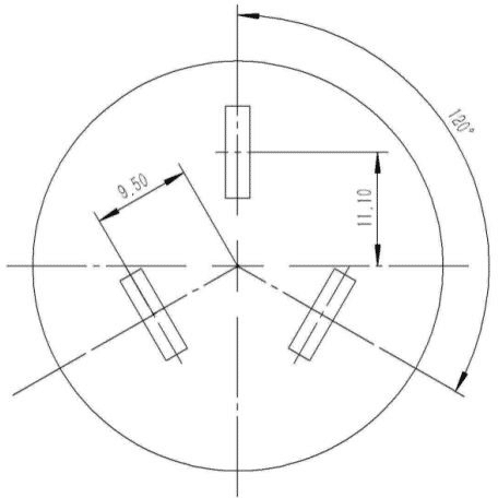
The inner diameter of standard specimen chamber is Φ 156mm; inlet diameter of the chamber is Φ153mm; the height of the chamber is 284mm.
The chamber can be equipped with various stages and detectors, such as X-ray wave dispersive spectr
ometer, X-ray energy dispersive spectrometer, Cathodoluminescence spectrometer, backscattered electrons detector, SE detector and other experimental instrument.The electron optical column and chamber must work on certain vacuum state. The realization and control of vacuum state can be completed by vacuum system. The automatic vacuum system is
Standard Specimen Stage
The standard specimen stage is applied to standard chamber. The range of movement is as follows:
- Horizontal X = Y=50mm
- Vertical Z=25mm
- Tilt=-5° ~ +90°
- Rotation= 360°continuously
For the needs of reduce vibration, specimen stage can be locked with specimen chamber by the interlock device.
Accessories of Standard Chamber
High temperature stage, low temperature stage and tensile stage can be installed in standard chamber for observing the state changes of specimen in different conditions.
Automatic Vacuum System
Installed under chamber, and directly connected with column through vacuum pipeline, which is shown below:

The automatic vacuum system mainly includes Turbo Molecular Pump, Mechanical Pump, Cold Cathode Gauge, connecting pipeline, damping device, various valves, and various gauges etc.
If you need more information about scanning electron microscope price and theory , please send email to [email protected].


Comments are closed.
Great post. I was checking constantly this blog and I am impressed! I care for such information much. I was seeking this certain info for a very long time.
It is evident that you have put immense effort into researching and presenting the information in this blog.
These well-researched and data-driven blog posts are a testament to your expertise in the field.
Hey, thanks for the blog.Really looking forward to read more. Cool.